Focus News
Smallest Stable Si/SiO2 Interface that Suppresses Quantum Tunneling from Machine-Learning based Global Search
Time:2022-05-07
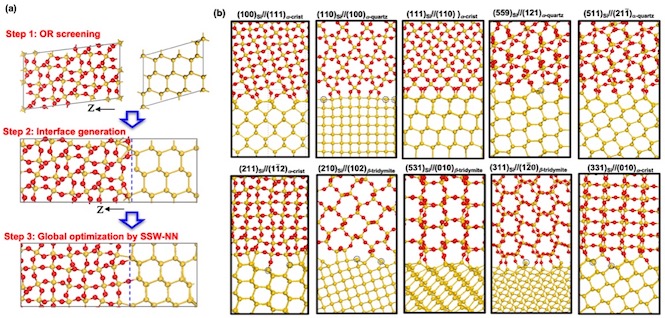
While the downscaling of size for field effect transistors is highly desirable for computation efficiency, the quantum tunneling at the Si/SiO2 interface becomes the leading concern when approaching to the nanometer scale. By developing machine learning based global search method, we now reveal all the likely Si/SiO2 interface structures from thousands of candidates. Two high Mill index Si(210) and (211) interfaces, being only ~1 nm in periodicity, are found to possess good carrier mobility, low carrier trapping, and low interfacial energy. The results provide the basis for fabricating stepped Si surfaces for next generation transistors.
https://journals.aps.org/prl/accepted/c8072Y0fW9211975a64c3939ac594d5c80d1af8d7

